A New Family of 2D Semiconductors Allows for More Energy-Effective Electronic Devices.
SUTD researchers demonstrate how a new family of 2D semiconductors is more efficient due to including an atomic protection layer.
Researchers from the Singapore University of Technology and Design claim that a new family of 2D semiconductors could open the door to high-performance and efficient electronics. These findings were published in 2D Materials and Applications. They could lead to the fabrication and use of semiconductor devices in mainstream electronics and optoelectronics and even replace silicon-based technology.
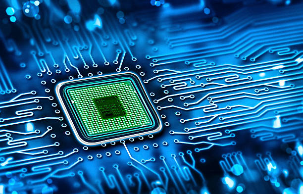
Moore’s Law is a well-known trend in pursuing miniaturizing electronic gadgets. It describes how the number and size of the components within integrated circuits of computers double every two years. This is possible due to shrinking transistor sizes, which can fit on chips as small as a fingernail. As this trend continues, engineers are beginning to confront the inherent limitations of silicon-based technology.
Professor Ang Yee Sin, SUTD Assistant, led the study. “Due to quantum tunneling effect,” he said. “People are looking for new materials beyond the silicon age’. 2D semiconductors are a promising option.
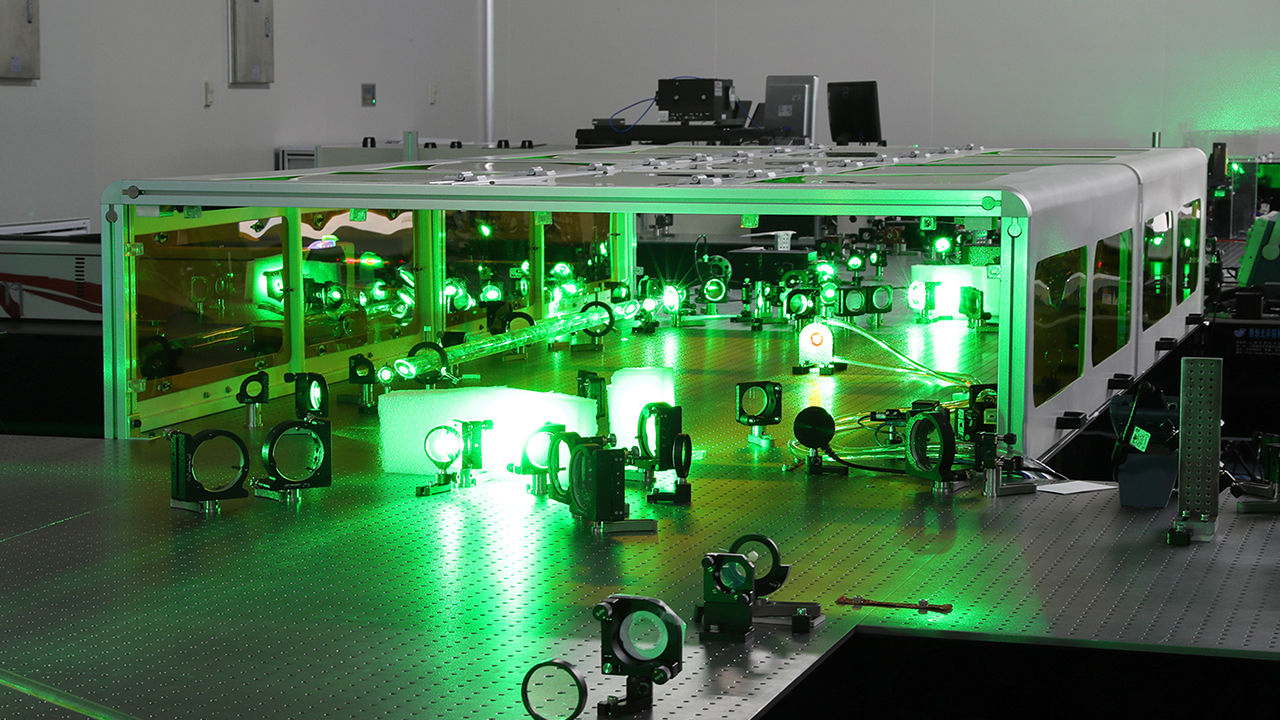
2D semiconductors are materials with a thickness of only a few nanometers. Because of their small size, these materials can be used as replacements for silicon. Unfortunately, most 2D semiconductors on the market are susceptible to high electrical resistance when in contact with metals.
Ang explained that Schottky barriers are formed when metal and semiconductors come into contact. It would help if you used a solid voltage to force electricity through the wall. This wastes electricity and creates heat.
The team was intrigued by Ohmic contacts, metal-semiconductor contacts with no Schottky barriers. Ang and collaborators from Nanjing University and Zhejiang University showed that a newly discovered family of 2D semiconductors, namely MoSi N 4 and WSi 2N 4, forms Ohmic contacts to the metals scandium, titanium, and nickel.
The researchers also found that the new materials were free from Fermi-level pinning (FLP), which is a problem that severely restricts the potential application of 2D semiconductors.
“FLP” is an adverse effect in many metal-semiconductor contacts and is caused by defects and complex material interactions at the interface. This effect “pins” the electrical properties to a narrow range, regardless of the metal used.
Because of FLP, engineers cannot tune or adjust the Schottky barrier between the metal and semiconductor–diminishing the design flexibility of a semiconductor device.
Engineers use strategies to minimize FLP. These include positioning the 2D silicon on top of the metal, creating a buffer between the semiconductor and the metal, or using a 2D metallic as a contact material for the 2D semiconductor. These methods may be feasible, but they could be more practical. They are also incompatible with mass production using mainstream industry techniques.
Amazingly, Ang’s team demonstrated that MoSi 2N 4 and WSi 2N 4 are naturally protected against FLP thanks to an inert SiN outer layer. This shields the semiconducting layer from material interactions and defects at the contact interface.
This protection allows the Schottky barrier to be ‘unpinned,’ which can be adjusted to suit various applications. 2D semiconductors are now in competition with silicon-based technology. Major players such as Samsung and TSMC have already expressed interest in 2D semiconductor electronics.
Ang hopes their research will inspire other researchers to explore more members of the 2D semiconductor family, looking for attractive properties.
He concluded that while some of these materials might not be suitable for electronics, others are good for spintronics and photocatalysts or as a building block of solar cells. “Our next task is to scan all these 2D materials and classify them according to potential uses.